1 0 0 Plane Fcc
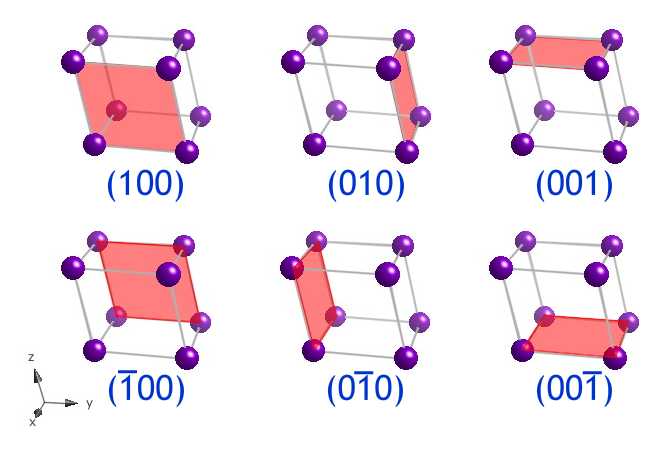
Doitpoms Tlp Library Lattice Planes And Miller Indices Examples Of Lattice Planes
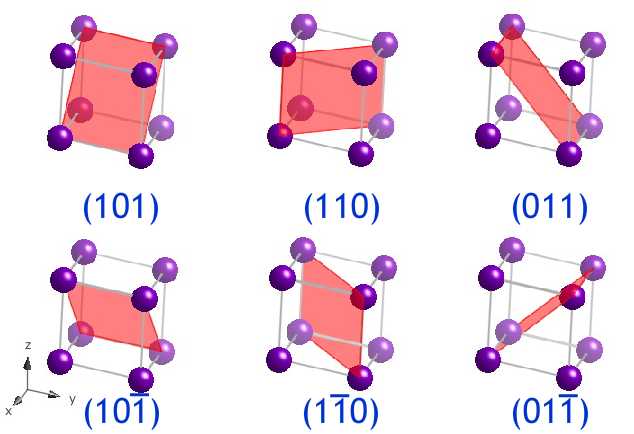
Doitpoms Tlp Library Lattice Planes And Miller Indices Examples Of Lattice Planes
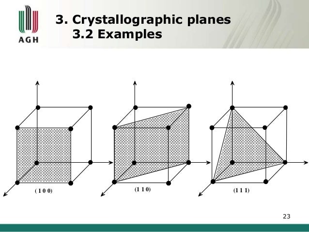
Crystallographic Planes And Directions
Crystallographic Points Directions Planes

Atomic Plane An Overview Sciencedirect Topics

Cubic Unit Cell An Overview Sciencedirect Topics
Crystallographic Points Directions Planes
Surface Structure Ii Crystal Structure Of Elements Bravais Lattices Miller Indices Weber Symbols Close Packing Fcc Hcp Bcc Stacking Faults Low Index Ppt Download
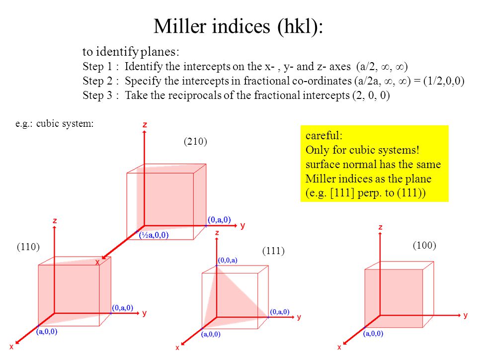
1 2 Miller Indices Hkl Chemistry Libretexts

Miller Index Wikipedia
Semiconductor Crystals Solid State Physics Britenyspears Ac

Miller Index Wikipedia
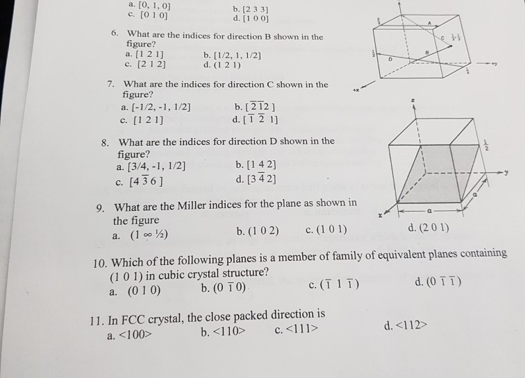
Solved B 233 D 1 0 0 C 0 10 6 What Are The Indi Chegg Com
Crystal Planes In Silicon Miller Index Angle Between Planes Wafer Flat Crystallography

111 Planes In Fcc Metal Youtube

Top Panel 1 0 0 Plane Representation Of The Facecentred Cubic Fcc Download Scientific Diagram

Crystal Planes In Semiconductors

A Crack Orientation B The Corresponding Fcc Planar Yield Surface Download Scientific Diagram
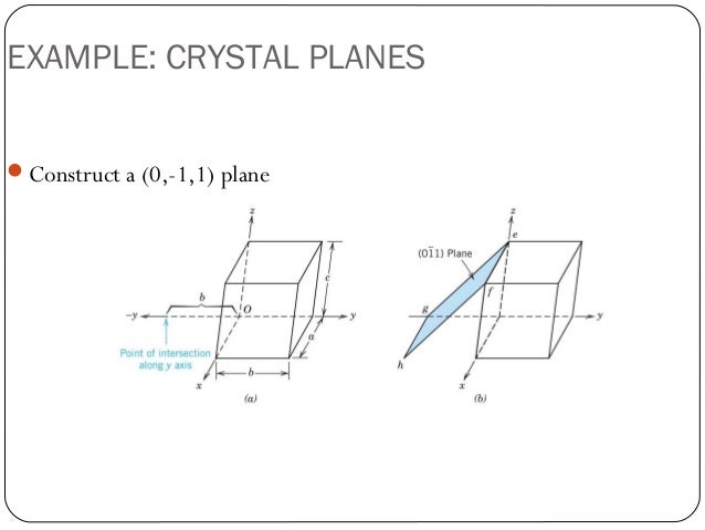
Unit2 Answer1
Https Web Iit Edu Sites Web Files Departments Academic Affairs Academic Resource Center Pdfs Crystal Structures Pdf
Source : pinterest.com