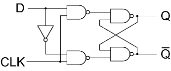
Circuit Diagram D Flip Flop Truth Table
Flip Flops In Electronics T Flip Flop Sr Flip Flop Jk Flip Flop D Flip Flop Circuits

D Flip Flop D Ff
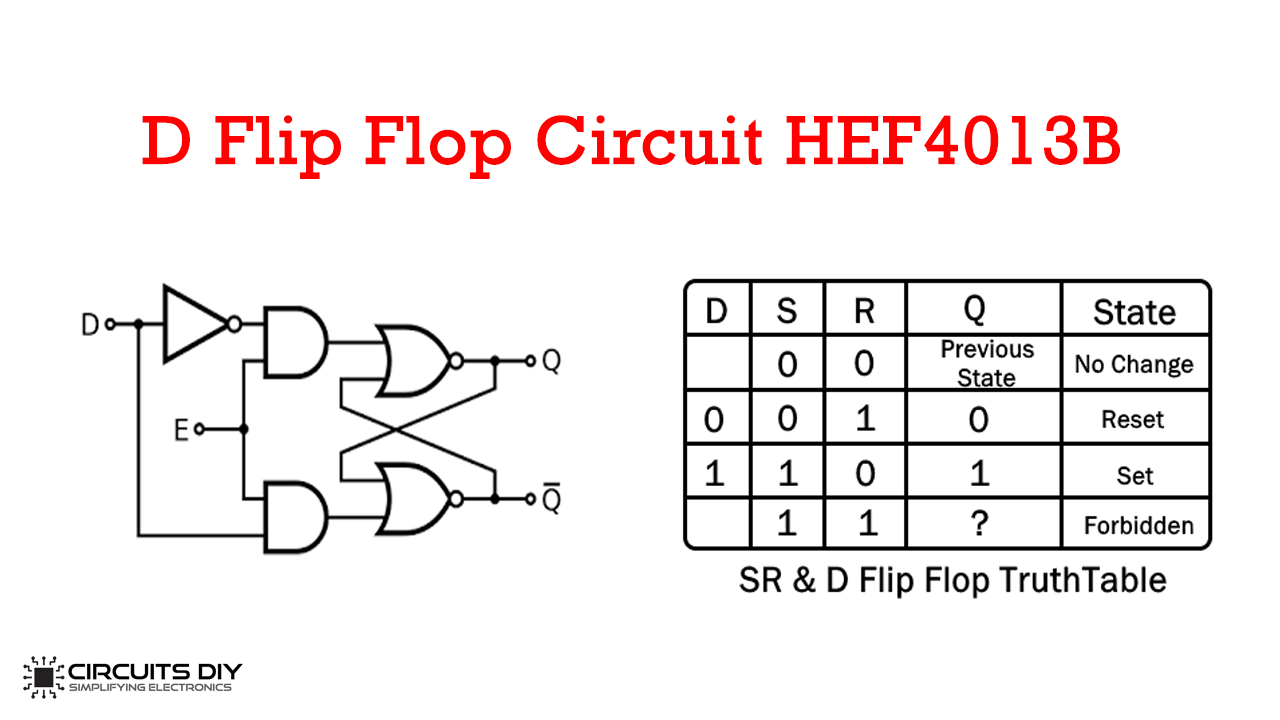
D Flip Flop Circuit Using Hef4013b Truth Table
Jk Flip Flop Diagram Truth Tables Explained Bright Hub Engineering
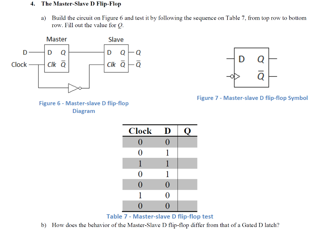
Solved 4 The Master Slave D Flip Flop Build The Circuit Chegg Com
D Type Flip Flops
The ic power source v dd ranges from 0 to 7v and the data is available in the datasheet.
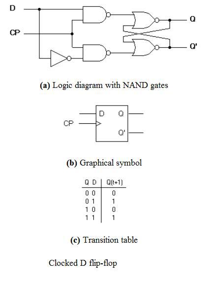
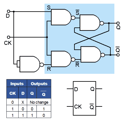
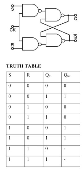
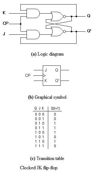
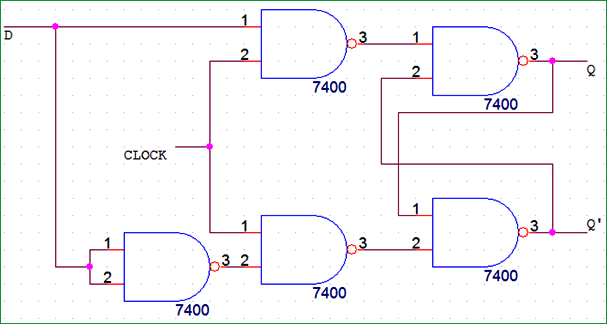
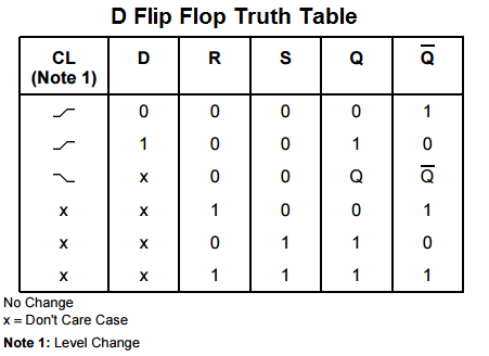
Circuit diagram d flip flop truth table. A flip flop on the other hand is synchronous and is also known as gated or clocked sr latch. From the figure you can see that the d input is connected to the s input and the complement of the d input is connected to the r input. Thus d flip flop is a controlled bi stable latch where the clock signal is the control signal. When both j and k are at logic 1 the jk flip flop toggle.
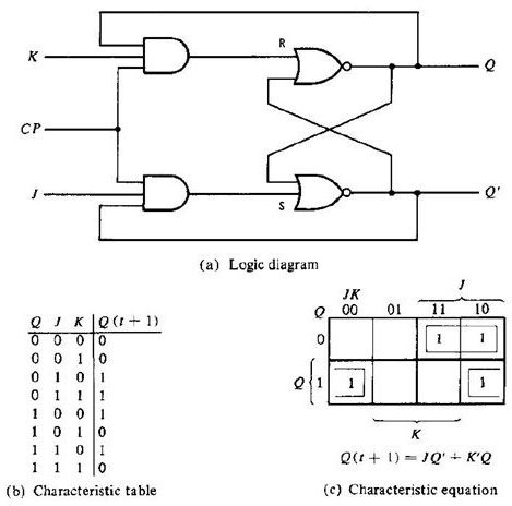
D flip flop is actually a slight modification of the above explained clocked sr flip flop. If the circuit is in the set condition the j input is inhibited by the status 0 of q through the lower nand gate. Jk flip flop circuit diagram and explanation. The karnaugh map solution of jk flip flop with.
Nor or nand gate can be used to make d flip flops out of which the nand gate is mostly used. Also we have used led at output the source has been limited to 5v to control the supply voltage and dc output voltage. These flip flops are simple in wirings and can only be used when the clock is set at high to get it activated. Truth table of jk flip flop.
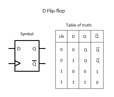
Truth table of d flip flop. Sr flip flop construction logic circuit diagram logic symbol truth table characteristic equation excitation table are discussed. The truth table of the jk flip flop is shown below. The tables above show us t he truth tables of jk flip flop with.
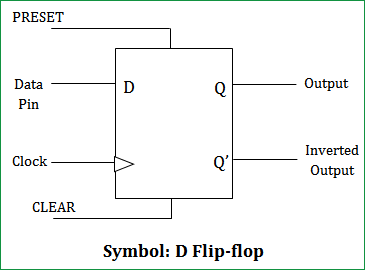
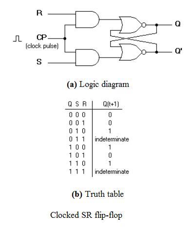
The stored data is changed only when you give an active clock signal. In electronics a flip flop or latch is a circuit that has two stable states and can be used to store state information a bistable multivibrator the circuit can be made to change state by signals applied to one or more control inputs and will have one or two outputs. Sr flip flop is the simplest type of flip flops. It is the basic storage element in sequential logic flip flops and latches are fundamental building blocks of digital.
Below snapshot shows it. The characteristic equations for the karnaugh maps of the figure above are respectively basic symbol and circuit diagram of jk flip flop. A active high inputs and b active low inputs. Similarly the input k is inhibited by 0 status of q through the upper nand gate in the reset condition.
Such flip flops are bi stabled latch and can further be divided into positive edge triggered d flip flop and a negative edge trigger d flip flop. In this circuit diagram the output is changed i e. Thus the output has two stable states based on the inputs which have been discussed below.
Transistor D Latch Does Not Latch Electrical Engineering Stack Exchange

Digital Teaching Aid Flip Flops Lesson 7 Lesson Plan D Flip Flop D Ff
Flip Flop Types Their Conversion And Applications Geeksforgeeks
Flip Flops In Electronics T Flip Flop Sr Flip Flop Jk Flip Flop D Flip Flop Circuits
D Flip Flop Circuit Diagram Working Truth Table Explained
D Flip Flop Circuit Diagram Working Truth Table Explained

Realization Of Negative Edge Triggered D Flip Flop By Proposed Rdff Download Scientific Diagram

Lr 2170 Flipflop Sequential Circuit Diagram D Flipflop Electrical Wiring Diagram
How To Build A D Flip Flop Circuit With A 4013 Chip

D Type Flip Flop Counter Or Delay Flip Flop
Flip Flops In Electronics T Flip Flop Sr Flip Flop Jk Flip Flop D Flip Flop Circuits

Jk Flip Flop And The Master Slave Jk Flip Flop Tutorial
Flip Flop Truth Table Various Types Basics For Beginners
